- 您现在的位置:买卖IC网 > Sheet目录1990 > BU2508FV-E2 (Rohm Semiconductor)IC DAC 10BIT 4-CHAN SSOP14
BU2508FV,BU2507FV
Technical Note
7/8
www.rohm.com
2011.08 - Rev.C
2011 ROHM Co., Ltd. All rights reserved.
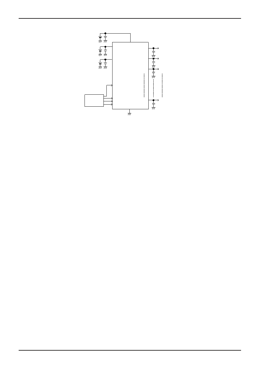
●Standard Example Application Circuit
●Notes for use
(1) The electrical characteristic and data on graphs for this datasheet, are typically evaluated value, and not guaranteed.
(2) We suppose that application circuits are recommendable, but please make sufficient check for characteristics with the
actual application. In case that value of external component for this IC is changed, please check characteristic, not only
static but also transient.
(3) About absolute maximum ratings
If operation condition is over the absolute maximum ratings, supply voltage or other operation range, IC will be broken.
Please don't apply any voltage or temperature over the absolute maximum ratings. If application have possibilities of
become over the absolute maximum ratings, please take safety measures by using fuse and so on. Not to over absolute
maximum ratings of IC.
(4) GND voltage
Please keep GND voltage lowest of any other terminal of this IC. Please confirm other terminal voltages is not lower
than GND.
(5) Thermal design
Please making a thermal design that allows for a sufficient margin in light of the power dissipation in actual operating
condition.
(6) About terminals short and wrong mounting
Please pay full attention to the IC direction and displacement when mounting IC on PCB. If you assemble them by
mistake and electrify it, IC might be destroyed. And it is happen to short among IC terminals or terminals and power
supply, by foreign substance.
(7) About operation in strong electromagnetic field
If you use it in strong electromagnetic field, please evaluate fully as there is a possibility of malfunction.
(8) Place a bypass capacitor as close as possible between each power supply terminal and ground in order to prevent
deterioration of the D/A conversion accuracy due to ripple and noise signals from power supply or GND.
(9) A capacitor should be inserted between the analog output and ground in order to eliminate noise.
A capacitance up to 100pF is recommended (including the capacitance of the wire).
AO 1
AO 2
AO 3
V refH
V refL
VC C
GND
AO 6
DI
CLK
LD
C ontro ller
CH1
CH2
CH3
CH6
Reset
发布紧急采购,3分钟左右您将得到回复。
相关PDF资料
BU3076HFV-TR
IC CLOCK GEN 1CH HVSOF6
CA3338AMZ96
IC DAC 8BIT 50MSPS R-R 16-SOIC
CDCR83DBQG4
IC DIRECT RAMBUS CLK GEN 24-QSOP
CDP68HC68T1M
IC RTC 32X8 NVSRAM CMOS 20-SOIC
CPLL66-1600-2200
IC VCO PLL/SYNTH 2.2GHZ SMD
CPLL66-2175-2175
IC VCO PLL/SYNTH 2175MHZ SMD
CPLL66-2400-2500
IC VCO PLL/SYNTH 2500MHZ SMD
CPLL66-2450-2450
IC VCO PLL/SYNTH 2450MHZ SMD
相关代理商/技术参数
BU2508-M3/45
制造商:Vishay Semiconductors 功能描述:25A,800V,STD,INLINE POWER BRIDGE
BU2508-M3/51
制造商:Vishay Semiconductors 功能描述:25A,800V,STD,INLINE POWER BRIDGE
BU-25094
制造商:Fema Electronics Corporation 功能描述:
BU2510
制造商:VISHAY 制造商全称:Vishay Siliconix 功能描述:Enhanced PowerBridge Rectifiers
BU25105S-E3/45
功能描述:桥式整流器 25 Amp 1000 Volt
RoHS:否 制造商:Vishay 产品:Single Phase Bridge 峰值反向电压:1000 V 最大 RMS 反向电压: 正向连续电流:4.5 A 最大浪涌电流:450 A 正向电压下降:1 V 最大反向漏泄电流:10 uA 功率耗散: 最大工作温度:+ 150 C 长度:30.3 mm 宽度:4.1 mm 高度:20.3 mm 安装风格:Through Hole 封装 / 箱体:SIP-4 封装:Tube
BU25105S-M3/45
制造商:Vishay Semiconductors 功能描述:25A,1000V,STD,INLINE POWER BRIDGE
BU2510-E3/45
功能描述:桥式整流器 25 Amp 1000 Volt RoHS:否 制造商:Vishay 产品:Single Phase Bridge 峰值反向电压:1000 V 最大 RMS 反向电压: 正向连续电流:4.5 A 最大浪涌电流:450 A 正向电压下降:1 V 最大反向漏泄电流:10 uA 功率耗散: 最大工作温度:+ 150 C 长度:30.3 mm 宽度:4.1 mm 高度:20.3 mm 安装风格:Through Hole 封装 / 箱体:SIP-4 封装:Tube
BU2510-E3/51
功能描述:桥式整流器 25 Amp 1000 Volt RoHS:否 制造商:Vishay 产品:Single Phase Bridge 峰值反向电压:1000 V 最大 RMS 反向电压: 正向连续电流:4.5 A 最大浪涌电流:450 A 正向电压下降:1 V 最大反向漏泄电流:10 uA 功率耗散: 最大工作温度:+ 150 C 长度:30.3 mm 宽度:4.1 mm 高度:20.3 mm 安装风格:Through Hole 封装 / 箱体:SIP-4 封装:Tube